
ParyIene's unique vapor-phase polymerization differs considerably from the application processes of other coating materials.
Key Points
Used as moisture and dielectric barriers, polymer parylene (p-xylylene/XY) coatings are conformal and pinhole free. Applied by a unique chemical vapor deposition (CVD) method, parylene penetrates beneath substrate facades, simultaneously attaching above surfaces at the molecular level. CVD generated films cover crevices, exposed internal regions, points and sharp edges uniformly, without gaps or breaches. Compared to liquid coating materials – acrylic, epoxy, silicone and urethane -- XY film layers are micron-thin, enhancing their utility for microelectricalmechanical systems (MEMS) and nano technology (NT).
At the same time, XY application is never flawless and needs to be carefully monitored. With CVD, deposition thickness is typically regulated by total quantity of solid-phase dimer loaded in the sublimation chamber at process commencement; process end-point occurs when dimer is exhausted. Thickness measurements are desirable because this CVD end-point can hinder precise, repeatable control of film thickness. The inaccuracy of predicting and controlling the deposition thickness is especially problematic when the deposition thickness is small (e.g., less than 1 micron). Film thickness appropriate to requirements of the coating assignment is key to reliable parylene performance.
Applied too thin, the coated device will be vulnerable to environmental risks – caustic fluids, chemical incursion, salt air, etc. – and malfunction. Too little parylene can mean incomplete coverage, pinholes, and reduced wear-ratings. In contrast, overly thick film application can generate:
XY polymers exist in a variety of types, including the Parylenes C, N, D, AF-4, and F. Each has its own range of chemical and performance properties, appropriate to precise coating functions. Measurement of coating thickness is essential to assure the specific XY type is applied at proper thickness for optimal operation. Measurement helps maximize the benefits of parylene coatings, including biocompatibility, high reliability, light weight, stress-free impact, and transparency. Typically, coating thickness is specified according to the material used for the film, and the function of the particular assembly.
Calipers can be used to measure the coated device, recording its dimensions across various areas of its topography prior to CVD. Re-measuring the same regions after CVD will show coating thickness, defined as the difference from the original reading. The film’s uniformity of application is assessed by standard deviation analysis. Coating both sides of a device is common with parylene; division of the total by two provides reliable measure of the film’s thickness on all sides.
Test coupons (TCs) economically and accurately measure coating thickness. Sprayed onto substrates both prior to- and following a production run, TCs register a device’s size for each condition. Ideally, they are composed either of the same material as the coated device; otherwise non-porous materials like glass or metal, are used. A test probe set flat on the XY film’s surface produces measures accurate to ±1 um, for films as thin as 25-50 um. Micrometers or similarly dependable instruments compare finished coating to assure quality specifications; non-contact techniques use eddy currents.
With different chemical and optical properties, refractive indexes (RI -- dispersion of XY material) of each parylene varies, often significantly. Algorithmic estimates of coating thickness are convenient in the production environment, but if RI is unknown, the thickness reading will be inaccurate. Highly variable, this method is not suited for applications requiring critical thicknesses. Precise thin film depositions require commensurately precise measurement tools in real-time, according to reliably calculated parylene-to-substrate thickness ratios.
Optical reflectometry offers accurate and verifiable measurement and control of film thickness(t) for XY coating systems.
Monitoring thickness levels during application requires balancing the total number of cycles during XY application with the fraction of cycles measured, based on a pre-determined standard for film thickness for that coating run.
Accurate and precise control of coating thickness is essential to successful target fabrication. Recently devised in-situ sensors working from thermal transfer principles end CVD when a targeted thickness is achieved. The device consists of a temperature sensor and a heater split by a well-defined gap, defined as d. When CVD reaches one half d’s value, d/2, the heat conducts through both the gap and the substrate. The thermal signature determines the gap-closing event, stopping CVD. The sensor measures both the quantity of parylene dispensed and its film thickness as deposited on the substrate, signaling CVD completion at specified thickness. This method both manages and measures XY deposition thickness, with a functional efficiency improving the +/- 10% of desired thickness standard often used, making it far more desirable for MEMS/NT applications.
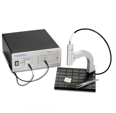
The Filmetrics F3-CS system is an exceptional instrument for measuring parylene thickness, specifically designed for XY films applied on flat surfaces, to measure small witness or coupon samples. USB-powered F3-CS acquires reflectance data via a contact stage that maintains the same working distance of the measurement sample throughout the process, in the following manner:
The optical constants (n and k) for Parylenes C and N layers are fundamental components of F3-CS, powered by any computers running Windows XP® through 64-bit Windows 8®. Presented in real-time, thickness results can be upgraded to measure refractive index.
Other Filmetrics products calibrate parylene thickness for curved surfaces and coatings exceeding the 0.25-75 microns standard. Diamond MT uses Filmetrics equipment for measurement purposes.
How it Protects
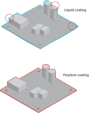
Parylene (XY) polymers provide robust, dielectric, micron-thin conformal coatings for a considerable range of electronic devices, most prominently printed circuit boards (PCBs). XY’s unique chemical vapor deposition (CVD) application method synthesizes in-process, depositing gaseous parylene deep into a substrate’s surface. CVD occurs on a molecule-by-molecule basis, conforming to all underlying contours, regardless of shape or position, to the nanometer, if necessary. Pre-synthesized liquid coatings lack many of parylene’s performance properties, having far less ability to successfully and conformally penetrate crevices in the substrate
Additional CVD advantages include:
Although there are two basic kinds of parylene dimer -- C and N -- other formulations exist – including D, F and HT. Each displays specified performance metrics, characterized by different electrical and physical properties.
Of parylene types, Type HT has the highest penetrating ability, as well as the lowest coefficient of friction and dielectric constant. It is also expensive to make and used essentially for specialized purposes, limiting its application for a wide range of conformal coating assignments.
Of the more common XY varietals, Parylene N is the base structure of the parylene group, offering a higher dielectric strength than C, F or D. In addition, it penetrates crevices and other cracks or gaps in substrate surfaces more capably than the others. Type N does this because enhanced molecular activity occurs during CVD, in comparison to the remaining XY varieties, allowing more efficient coating of relatively deep recesses, blind holes, tubes and small openings.
Parylene C is used more frequently than any other XY variety. It offers better performance across most metrics, generating exceptional protection from corrosive gases, due to low chemical, moisture, and vapor permeability. Depositing quickly on most substrate surfaces, C’s lesser throw-capability can reduce crevice-penetration activity; it provides lesser crevice penetration than Type N.
With chlorine atoms added to its benzene ring, Parylene D film has greater thermal stability than N, F or C. Crevice penetration capacities are lower in comparison to other XY varietals.
With a chemical structure of four fluorine atoms on the aromatic carbons, Type F provides good crevice penetration. Its dimer is also very expensive, limiting its use for many conformal coating projects.
CVD processes convert powdered parylene dimer into a vapor; the resultant coating substance responds with reliable conformability to surface geometries, including:
Only XY offers this level of adaptability to highly complex coating problems, generating precise conformance to substrate topography without bridging or pooling. Applied in micron-thin layers, parylene's pinhole-free coverage penetrates and coats complex surfaces to a degree impossible with liquid conformal film materials.
Ultimately, CVD is responsible for XY’s exceptional crevice penetration.
In any case, the gap is filled with a durable, micron-thin parylene conformal film, regardless of surface complexity.
Quality Standards
Parylene conformal coating (XY) provides insulative protection for complex electronic circuit assemblies expected to function through rigorous operating conditions -- potential chemical, electrical, moisture and vapor incursion during performance. Applied through chemical vapor deposition (CVD), parylene penetrates deep within substrate surfaces, generating a level of assembly security surpassing that offered by liquid coatings such as acrylic, epoxy, silicone and urethane. Yet, although XY is applied in a vacuum, it’s capacity to provide these extraordinary qualities does not exist in one. Parylene’s durable protective value depends on film adhesion, a quality subject to persistent, thorough inspection throughout the production process.
Diamond MT’s parylene services include coating provision for clients’ printed circuit boards (PCBs), medical devices, and similar products, shipped to our production facility. The incoming inspection process begins immediately after items awaiting parylene coating have been unpacked:
Individual processing follows these procedures, with additional inspection and cleanliness testing. This is imperative; substrate contaminants may have accumulated during manufacture, handling and transportation. Without question, the most significant factor affecting parylene (or any conformal coating) adhesion is surface cleanliness; contaminated surfaces lead to poor coating quality, limited adhesion, and delamination, defeating the purpose of XY application. To this degree. cleanliness inspection is a vital step in the parylene coating process, assuring the substrate surface is ready to accept parylene conformal coating without incident.
Visual inspection alone is insufficient to confirm a PCB’s suitable cleanliness and other stage-readiness for XY coating. Throughout the production-run, every phase of the process must be consistently measured and monitored; this ongoing performance inspection averts costly cleaning issues. At Diamond, we maintain a sampling process throughout each production run, designed to:
According to IPC-J-STD-001 specifications, surface cleanliness levels should register 10µgm NaCl/in2 or less. Diminishing adherence to this standard is inadvisable; doing so jeopardizes coating and assembly performance. Substrate contamination undetected prior to film application requires process-cessation, and substrate recleaning, until acceptable non-contamination levels are achieved. These costly missteps are avoided by appropriately implemented cleanliness inspection before XY application is commenced.
XY inspection for quality assurance also details the degree of the coating thickness necessary to meet assignment specifications, PCB-area of coverage, visual, and adhesion-testing requirements. Subject to intensive inspection and evaluation, micron-thin XY-films are constructively measured:
Quality attributes for parylene typically specify the use of various inspection procedures that verify appropriate surface purity. These include:
Once cleaning has been enacted, masking processes assure parylene coating doesn’t penetrate assembly keep-out areas, in accordance with client specifications. Subsequent masking inspection verifies compliance, leading to implementation of CVD procedures (the parylene coating process). After XY deposition, masking materials are removed, and the batch is subject to further inspection, to assure even, pinhole free coating without tears along formerly masked regions. Thickness inspection verifies appropriate film thickness has been achieved.
Prior to packaging coated assemblies, final inspection is necessary. Encompassing every aspect of the product, this process ensures
After passing final inspection, assemblies are ready to ship. At Diamond, return-to-client typically takes about ten business days, but faster turn-around can be negotiated at your request.
Parylene Chemistry and Production Requirements
ParyIene's unique vapor-phase polymerization differs considerably from the application processes of other coating materials. More complex, the technique deposits the substance directly onto the material being coated in a manner that penetrates deeper into the substrate surface. Implemented in a specialized vacuum chamber, parylene's application process does away with the intermediate liquid deposition procedure common to competing coatings.
Chemically, the various parylenes' main-chain phenyl group generates reliable molecule-to-molecule interaction, while possessing high levels of in-plane electronic polarization capabilities. Because these molecular layers are room temperature and chemical vapor deposited (CVD),
Thus, parylene's molecular layers are particularly valuable for microelectomechnical systems (MEMS) and nanotechnology driven applications, which emphasize simplifying component manufacturability.
Unfortunately, compared to other coating options, more time is generally needed to assure parylene's superior conformal coating of targeted substrates, a consideration that needs to be an integral component of manufacturing strategies. For instance, the fact that coating thicknesses from 0.10 micron to 76 microns can be applied in a single operation enhances the quality of completion of manufacturing processes. In general, however, slower production time leads to:
Parylene Deposition Rates and Process Duration
Parylene's application process is rather different and, in consequence, slower and more expensive than the traditional wet chemistry coating methods used for acrylic, silicone and other substances. The parylene process is multifaceted, involving several steps. Unlike many competing application processes, parylene deposition is not line-of-sight. Rather, the gaseous monomer uniformly encapsulates all sides of the object being coated simultaneously.
While CVD generates the truly conformal nature of parylene coating, it can be considerably slower to implement. In addition, appropriate cleaning, activation and masking precede CVD coating in the deposition chamber. Deposition rates for parylene conformal coating vary, often significantly, according to:
At Diamond MT, our processes are explicit, both in terms of the sequenced-procedures applied to every customer order, and adaptation of those procedures to precise customer specifications throughout the coating process. This may add to completion time, but the quality of results is unsurpassed and verifiable. Individual processes are enacted following inspection of incoming materials, including appropriate component cleaning and masking; at all times results of our in-house procedures are measured against customer diagrams to assure compliance with specification requirements. Adhesion management is also implemented, as necessary, before the coating cycle begins.
Because of these factors, processing time similarly varies, from less than an hour to 24 hours or more, figured at a standard deposition rate of about .2 mils-per-hour, a slower speed compared to the liquid application technique employed by the majority of other coating materials. Special care is taken to match parylene thickness to the product's specified coating requirements. Time to completion of the parylene coating process varies according to deposition rates: coating of lesser thickness will require less time to complete; thicknesses in excess of .2 mils-per-hour will require more time to complete, according to the desired thickness.
Conclusion
Biologically and chemically inert, parylene responds well to the CVD process. Not requiring the liquid phase application standard from most competing coating materials, parylene provides an authentically conformal covering. The excellent barrier strength is characterized by a completely pinhole-free and uniform thickness. Coating application is controllable at thicknesses > 0.5µ, while effectively penetrating product spaces as narrow 0.01mm, making parylene highly relevant to MEMS/nano uses.
Confirmation of these standards is as important to Diamond as it is to our valued customers, and contributes to production time. However, the attention paid to quality throughout all stages of the parylene coating process engenders enhanced delivery of client expectations. It simultaneously generates substrate coatings guaranteed to maintain component protection and performance for the duration of its expected operational life.
A Comparison
Parylene and acrylic resins are both conformal coatings. Most of the similarities stop there. Because their properties vary so much, they have their own unique uses and capabilities.
Application
Acrylic conformal coatings are a liquid conformal coating and can be applied four ways: spray, dip, brush, or robotics. Which method selected will vary by a couple of factors including: Quantity of products, complexity of masking requirements, and skill level of operators. They are usually applied between .002" and .005".
Parylene coating is applied through a vapor deposition process onto the substrate or material that is being coated. Depending on the coating type and required thickness, typical parylene deposition rates are about .2/mils per hour, so machine runs can vary from as little as 1 hour to over 24 hours. The process begins with raw dimer in solid state (these are: Parylene C, Parylene N, Parylene D, Parylene AF-4, or other variants) being placed into a loading boat, which is then inserted into the vaporizer. The raw dimer is heated between 100-150º C. At this time, the vapor is pulled, under vacuum into the furnace and heated to very high temperatures which allows for sublimation and the splitting of the molecule into a monomer. The monomer gas continues to be drawn by vacuum one molecule at a time onto the desired substrate at ambient temperatures in the coating chamber. The final stage of the parylene deposition process is the cold trap. The cold trap is cooled to between -90º and -120º C and is responsible for removing all residual parylene materials pulled through the coating chamber. As you can see, the application process of parylene is quite different than a traditional wet chemistry coating like acrylics.
Parylene films are usually applied between .0005” and .002”, but can be applied as little as .0001".
Common Uses
A common use of acrylics is on printed circuit boards for moisture protection.
While parylene can be used on printed circuit boards, it has a wide range of uses in medical products such as stents, catheters, and needles.
Disadvantages
In applications that have an exposure to solvents, acrylic conformal coating is not the best choice. Acrylic conformal coating can be removed with a weaker solvent such as isopropyl alcohol or xylene. Whenever it faces even stronger solvents, it will not offer the protection that is needed, especially if your product is a mission critical device.
For products that require a high temperature application, acrylic coatings will fall short of expectations. For HumiSeal 1B31, arguably the most popular acrylic coating, the max continuous operating temperature is 125ºC. Compare this to silicone conformal coating, whose operating temperature can exceed 200ºC.
One disadvantage of parylene is cost. The cost for parylene is typically higher than other conformal coatings. This is because of many factors, such as the process itself, the raw materials involved, and the labor required to properly prepare a device for coating. While this is not necessarily true for all applications, typically for an item quoted in parylene and wet chemistry, the parylene pricing will be higher.
Another major issue that comes up often for several of our high volume manufacturers is the limited throughput of parylene. Runs of the parylene machine can take anywhere from eight to over twenty-four hours. As a result of the limited chamber space, there is a fixed amount of product that can be processed during one coating cycle. This, coupled with the high capital cost of new equipment, can wreak havoc with our internal and our customer’s delivery schedules.