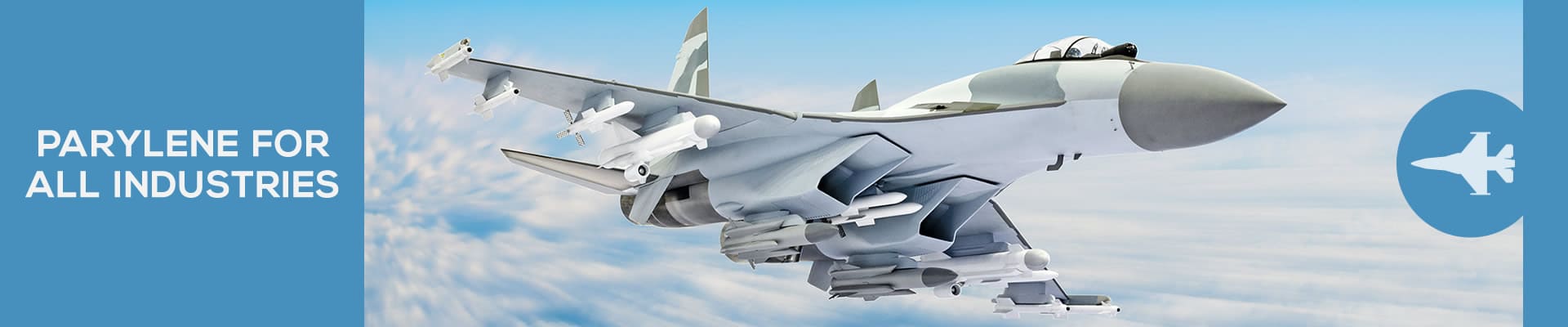
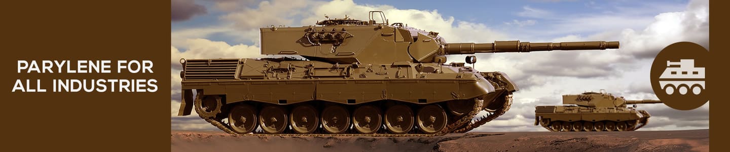
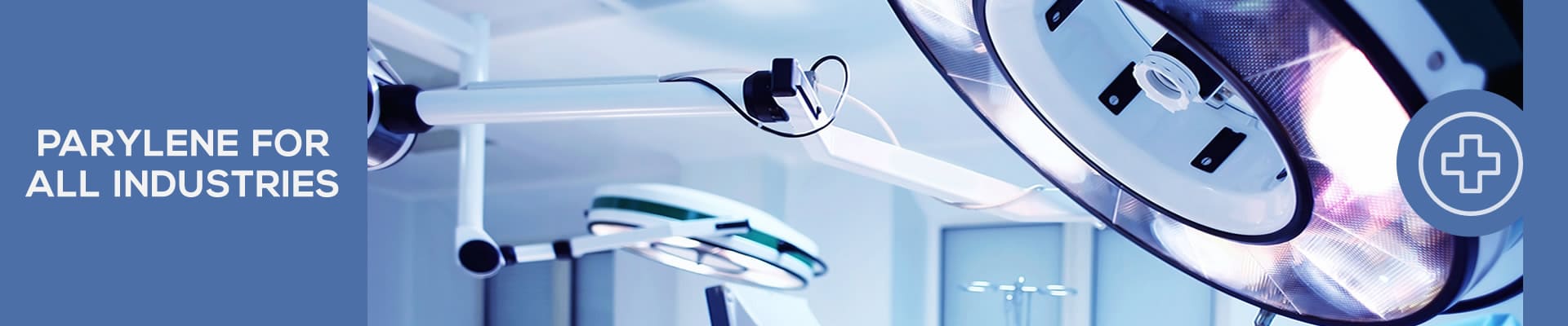
Parylene conformal coating is becoming an ever increasing part of everyday life for the defense, bio-medical, and other industries. Download Diamond-MT's Parylene 101: Coating Facts Sheet to understand the basic facts on the process.
Receive your instant download of the Parylene 101 Guide now by filling out this simple form.
Our process is clear and straightforward, ensuring the best possible end product.
Lorem ipsum dolor sit amet, consectetur adipiscing elit. Ut at interdum purus. In lorem lectus, luctus id lorem at, suscipit aliquam leo.

Lorem ipsum dolor sit amet, consectetur adipiscing elit. Ut at interdum purus. In lorem lectus, luctus id lorem at, suscipit aliquam leo.
Lorem ipsum dolor sit amet, consectetur adipiscing elit. Ut at interdum purus. In lorem lectus, luctus id lorem at, suscipit aliquam leo.
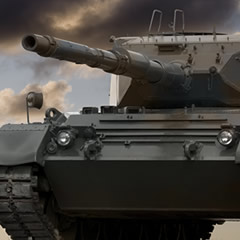
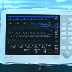
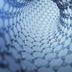
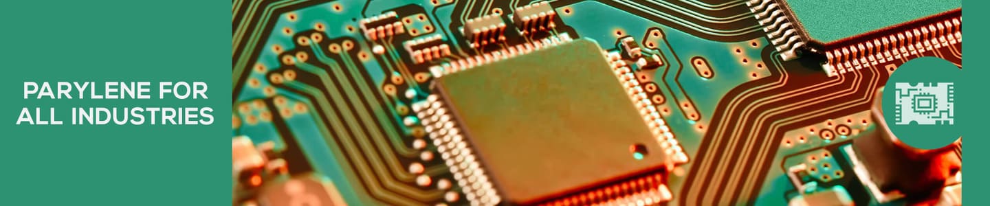
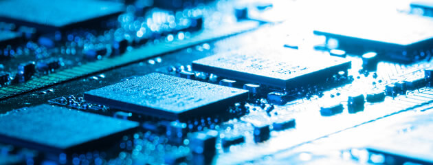
Parylene is considered by many to be the ultimate conformal coating for protection of devices, components and surfaces in electronics, instrumentation, aerospace, medical and engineering industries. Parylene is unique in being created directly on the surface at room temperature. It is chemically stable and makes an excellent barrier material, has excellent thermal endurance, as well as excellent mechanical properties and high tensile strength.
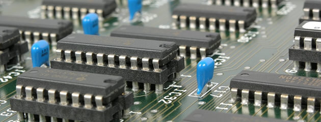
Here is a brief list of some of the items that can be parylene coated:
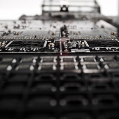
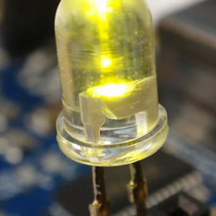
| Printed Circuit Boards | MEMs | LEDs |
| Catheters | Stents | Magnets |
| Paper | Needles | Sensors |
| Ferrite Cores | Metallic Blocks | Optical lenses |
| Implantable devices | Valves | O-rings |
| Tubing | Silicon Wafers | Keypads |
| Stoppers | Seals | Mandrels |
| Molds | Motor Assemblies | Power Supplies |
| Backplanes | Photoelectric Cells | Forceps |
| Test Tubes | Probes | Fiber Optic Components |
| Pace-makers | Bobbins | Plus Many More... |
Relatively easy to understand, the parylene deposition process can be difficult to implement, particularly with respect to controlling coating-thickness and otherwise ensuring a successful coating cycle.
Because coating type and required surface thickness vary according to substrate material and coating-project, deposition rates fluctuate. Processing can require less than an hour or more than 24 hours, at a deposition rate of about .2/mils-per-hour. While this slower rate of substrate covering generates parylene's superior conformal coating, compared to other coating options, it also adds to its cost. Mastering the parylene coating process helps assure these production expenditures are diminished.
Parylene's complex and specialized vapor-phase deposition technique ensures the polymer can be successfully applied as a structurally continuous film, entirely conformal to the characteristics of the selected substrate. To correctly master the process, assure each incoming order possesses all pertinent information affecting parylene application. This will include drawings, specifications, and special instructions that distinguish the order from others, allowing creation of customized solutions for the particular item.
Parylene's deposition process completely eliminates the wet deposition method used by such other coating materials as epoxy, silicone, or urethane. It begins in a chemical-vacuum chamber, with raw, powdered parylene dimer placed in a loading boat, and inserted into the vaporizer. The dimer is initially heated to between 100º - 150º C, converting the solid-state parylene into a gas at the molecular level. The process requires consistent levels of heat; the temperature must increase steadily, ultimately reaching 680º C, sublimating the vaporous molecules and splitting it into a monomer.
Drawn by vacuum onto the selected substrate one molecule-at-a-time in the coating chamber, the monomer gas reaches the final deposition phase, the cold trap. Here, temperatures are cooled drastically to levels sufficient to remove any residual parylene materials pulled through the coating chamber from the substrate, between -90º and -120º C.
Mastering the parylene coating process requires detailed attention to these procedures, prior to commencement of deposition and coating:
Thorough inspection of incoming items to-be-coated, verifying their quantity and condition. Preparation procedures enacted as necessary. For instance, cleaning/cleanliness-testing, or similar unique processes, are commenced, followed by masking of connectors and electrical components. Accumulated substrate contaminants diminish adhesion, so assuring appropriate levels of surface cleanliness is integral to parylene coating. Depending on the substrate surface, cleaning may be enacted manually, or through application of batch, inline, or ultrasonic methods. Most materials--glass, metal, plastic, etc.--require treatment with A-174 silane to effect appropriate surface modification before parylene application. Typically, doing so employs either manual-spray, soaking, or vapor-phase technology, applied after the masking operation, A-174 silane's molecule forms a unique chemical bond with the substrate's surface, sufficient to improve parylene adhesion.
Masking is exceptionally labor-intensive. Exceptional care is required to ensure every connector is effectively sealed, so gaseous parylene molecules do not penetrate their surfaces. All tape, or other covering materials, must thoroughly encompass the keep-out regions, without gaps, crevices or other openings, to ensure connector function is retained after coating.
Further inspection assures masking is in compliance with customers' specifications.
The diversity of adhesion promotion methods requires a similarly diverse list of raw materials. Establishing best-adhesion practices is only part of mastering the parylene coating process; once established, strict adherence standards need to be reliably enforced to ensure quality of the conformal coatings. Using industry best practices, such as substrate cleansing and A-174 silane application, appropriately combined with standard, repeatable processes, will ensure strong adhesion for parylene coating. Adhesion promotion methods are typically used prior to the actual coating process, however some can be integrated during the process itself.
The parylene coating is applied through the deposition process described above. Once coating has been deposited, masking materials are removed; extreme caution must be exercised not to damage the thin layer of applied parylene.
An important consideration of appropriate parylene thickness is total required clearance. While an enclosure-PCB has few clearance issues, in many cases even an additional millimeter of parylene coating can be sufficient to generate dysfunctional mechanical abrasion, damaging the parylene surface and reducing its conformal qualities.
Regarding dielectric strength, items whose required levels of dielectricity are higher will need a thicker coat of parylene. Balancing dielectric strength with clearance generally requires quality testing to determine their correct ratio. The end-item customer may not always provide these specifications; learning how to determine dielectric/clearance ratios without this data is integral to mastering the parylene deposition process.
The coating process must generate a conformal covering explicitly meeting the customer's precise specifications. If changes are necessary, making them to order and on time are essential elements of mastering the parylene coating processes. A final inspection ensures successful completion of all process phases, and that the final product complies with the customer’s drawings and specifications.
The raw material, parylene dimer, is rather expensive ranging from $200-$10,000+ per pound. Because parylene is applied through a vapor deposition process, everything, including items that do not need to be coated like inner diameter of the chamber, gets coated. This makes parylene an inherently inefficient process and wasteful with materials, which escalates the end cost to the customer.
Masking and otherwise prepping an article for parylene coating can be a labor intensive affair. Because parylene is applied as a vapor, it literally gets everywhere that air can. Our operators and quality inspectors must take this into account prior to coating to ensure that every one of the customer’s coating free areas are just that.
One major issue that often comes up for several of our high volume manufacturers is the limited throughput of parylene. Runs of the parylene machine can take anywhere from eight to over twenty-four hours. As a result of the limited chamber space, there is a fixed amount of product that can be processed during one coating cycle. This, coupled with the high capital cost of new equipment, can wreak havoc with our internal and our customer’s delivery schedules.
One final disadvantage of parylene to consider is the poor adhesion to many metals. Parylene has always had poor adhesion to gold, silver, stainless steel and other metals. Many printed circuit board manufacturers use gold in their products because of its conductivity. While there are some adhesion promotion methods that will greatly improve adhesion to these metals, they are either material or labor heavy and can increase costs significantly.
Parylene coating removal can be broken down into three categories for removal of parylene coating:
1) Chemical Removal: Parylene coatings are sought after primarily for their chemical resistance. Parylene resists room temperature chemical attacks and are insoluable in all organic solvents up to 150C. Thus parylene is highly chemical resistant and no chemical can dissolve it at room temperature.
However, Tetrahydrofuran is an organic solvent that can soften the coating, temporarily loosening the adhesion bond between the coating and the substrate so that it can be lifted off, like a mask, with tweezers. It is not suited to working with specific areas; in the case of rework and repair this is usually desired. It is highly flammable, caustic and extreme measures must be taken to ensure safe use.
2) Thermal Removal: All parylene variants demonstrate heat-resistance or "melting point" constraints for removal purposes ranging from 290C for parylene C, the most commonly used variant, to temperatures approaching 500C for parylene D, N, and F. A high quality soldering iron under a vacuum hood could be used to burn off at the solder points. This approach might be effective for small repairs though it is not the cleanest method. Along with residues, discoloration may pose a risk to heat sensitive components or substrates.
Laser ablation removes material from the surface by irradiating it with a laser beam. The beam can drill, cut, or mark delicate materials with great precision and repeatability.
Laser ablation removes very precise areas and tends to fit high density difficult to mask parts. Applications such as microelectronics, electrosurgical devices and implantable elctrodes that require very small, precise and intricate shapes to be free would be ssuited to this approach. It is less likely to be used for the purpose of general rework as it can be cost restrictive.
3) Mechanical Removal: Parylene demonstrates poor resistance to abrasion. Parylene is a soft polymer and as such physical or mechanical means is the best method for removal. Using coarse methods such as picking, scraping and cutting can be effective but there is a risk of damage to delicate trace lines, solder pads, components and the substrate itself.
The most common method to remove parylene is via micro-abrasion. This is the fastest, economic, and ecologically safe method for both spot and whole board parylene coating removal. Various media from glass beads, plastic beads, sodium bicarbonate, and wheat starch have been tested and used. Everything from complex to desktop equipment are available and can be used with a hand held stylus directing pressurized air and abrasive media.
Once the section is repaired, the specific area could be covered with other protective material. However, for optimum protection the whole board should be recoated with parylene.
There is no liquid phase involved. Coatings are truly conformal, of uniform controllable thickness, and are completely pinhole-free at thicknesses greater than 0.5µ.
Parylene coating completely penetrates spaces as narrow 0.01mm.
Parylene coating has excellent mechanical properties, including high tensile strength.
Parylene coatings are completely conformal, have a uniform thickness and are pinhole free. This is achieved by a unique vapor deposition polymerization process in which the coating is formed from a gaseous monomer without and intermediate liquid stage. As a result, component configurations with sharp edges, points, flat surfaces, crevices or exposed internal surfaces are coated uniformly without voids.
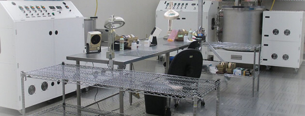
The parylene coating process is controlled via a programmable logic controller. Each deposition system features an operator’s control panel that displays critical, factory pre-programmed process parameters. Process settings are accessible and can be changed by qualified personnel when necessary. All machines feature closed loop monomer pressure control, ensuring deposition of the polymer film at a precise rate. All operating temperatures and pressures are continuously monitored and any deviation from the acceptable limits results in audible and visual alarms. Automatic process shutdown is initiated following process fault conditions of sufficient duration.
Diamond MT can help you discover the best equipment solutions for your specific needs. We work with you to ensure that you are getting the most cost effective solution for your product, whether that is parylene coating solutions, bringing equipment in house, or another type of conformal coating.
Parylene is stable over a very wide temperature range (-200 ‘C to +200 ‘C), allowing the chamber items coated in Parylene to be put in an autoclave.
FDA approval of parylene-coated devices is well-documented. The coatings comply with USP Class VI Plastics requirements and are MIL-I-46058C / IPC-CC-830B listed.
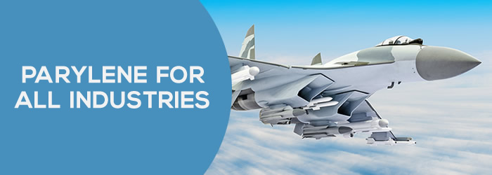
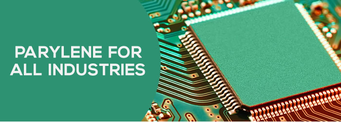
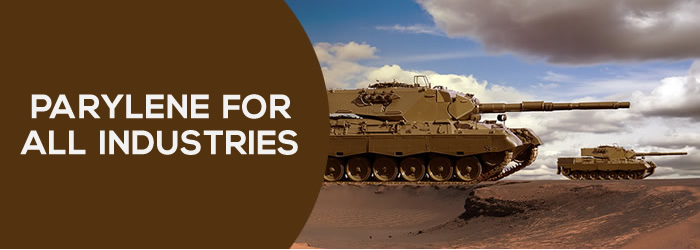
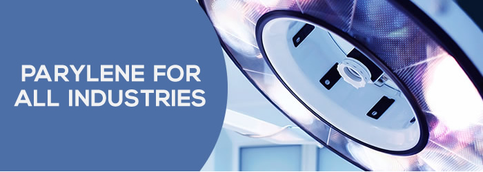
There are many different industries that conformal coating plays a critical role in.